Part 1 LCD: Using 2.4" TFT LCD Display (Without Library)
- Oct 6, 2021
- 9 min read
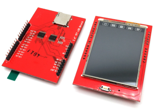
In this tutorial, we will be looking at how to use 2.4” Thin Film Transistor LCD 240RGB x 320 Resolution and 262K color without using any library.

The above shield can be easily topped over an Arduino UNO. Hence, there is no need to bother about pin arrangements or circuit setup. Just be gentle when connecting the LCD Display to Arduino to avoid breaking the pins of the LCD.
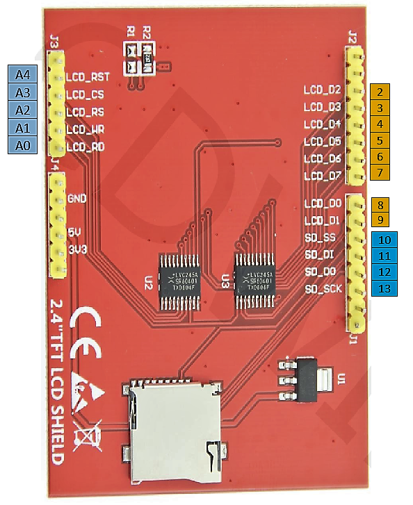
Figure below shows the pinout of the LCD module when connected to an Arduino UNO. The numbered pin boxes located outside of the figure shows the respective Arduino Pins when the shield connected is stacked on top of Arduino Uno.

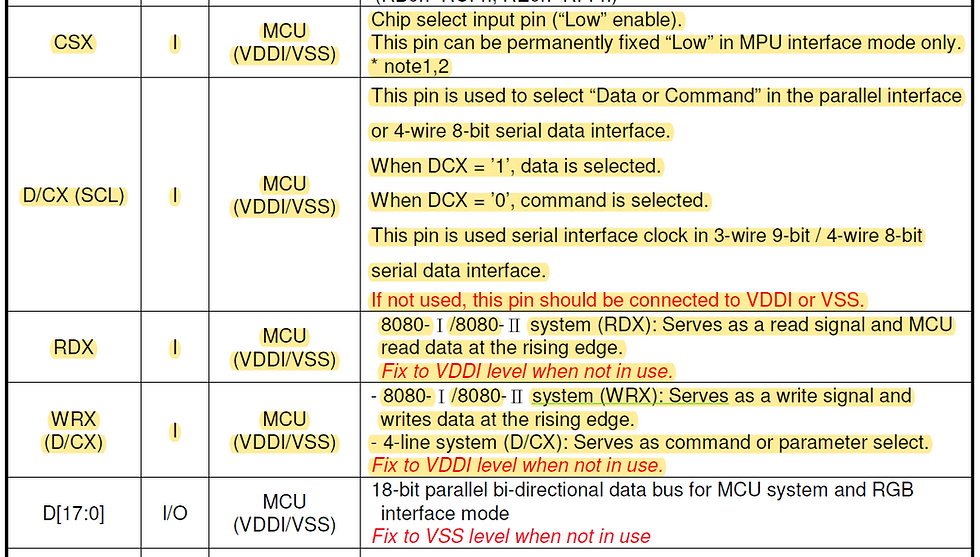
The table below shows the function of LCD_RST, CS, RS, WR and RD pins which are crucial in determining the behavior of LCD Display.

D/CX pin in table above is equivalent to RS pin from the LCD. D[17:0] refers to the Data Pin. DataPins from LCD Module refers to pin LCD_D0 to LCD_D7 which are 8 pins in total. These pins are connected to Arduino Digital Pin 2 – 9. For this tutorial, we are not utilizing the SD Card pins.
Now that we have identified the pins, let’s move to the next part to understand the behavior of LCD Display.
Refer the Write Cycle Sequence below.

Understand that when we are communicating a certain instruction to LCD Display from the microcontroller or Arduino UNO in our case, there will generally be two components to it; which are command and data. Command part will instruct the LCD on what instruction we’re working on, at a given time. For instance, setting colours and address, sleep, max and min voltage, LCD awake and sleep, write to memory and many more. Subsequently, we will send Data command which contains relevant or supporting information for the Command part that we sent earlier. It is also important to note, that some LCD instructions works using Command part alone in which we shall discuss the examples later.
The Write Cycle Sequence shown above tells us the state of LCD_RST, CS, RS, WR and RD when command or data is being sent. Note that :
Chip Select needs to be low as it is an ActiveLow Pin
D/CX or LCD_RS Pin is set to HIGH when sending the Command Part and LOW when sending the Data part
WRX or LCD_WR will write the Command and Data Part at every rising-edge signal
RESX or LCD_RST is set to HIGH
RDX or LCD_RD is set to HIGH
Now that we have a fair understanding on the behavior of LCD Display, we can move on to the coding part.
In the beginning of our program, we will have the below code :
#define BLACK   0x0000
#define BLUE    0x001F
#define RED     0xF800
#define RED2    0x4000
#define GREEN   0x07E0
#define CYAN    0x07FF
#define MAGENTA 0xF81F
#define YELLOW  0xFFE0
#define WHITE   0xFFFF
#define GREEN2  0x2FA4
#define CYAN2   0x07FF
The above code is just pre-defining some colors. We will discuss later on how did we come up the hex code for each color in detail. For now, just understand that the above colors are being represented by the hex code next to it.
#define LCD_RD   A0 //Serves as read signal/MCU read data at the rising edge. Pg11 Datasheet
#define LCD_WR   A1 //Serves as write signal/command at the rising edge
#define LCD_RS   A2 //D/CX (0=Command/1=Data)
#define LCD_CS   A3 //Chip Select Pin : Active Low
#define LCD_RST  A4 //Shield Reset
At this stage, we are defining our RD, WRX, D/CX, CS and Reset PIN from LCD to Arduino Analog Pins. This configuration is very crucial as assigning wrong PIN will result in almost guaranteed failure, hence be sure to double check. If you are using different type of shield or manually wiring the connections, then you can change analog PINS accordingly.
void LCD_write(uint8_t d) {
  // Serves as write signal/command at the rising edge
  digitalWrite(LCD_WR, LOW); // WR 0

  // LCD Pins |7|6|5|4|3|2|1|0|
  // Uno Pins |7|6|5|4|3|2|9|8|

  //Arduino Port D : Pin 0 - 7, but Pin 0,1 not used in the LCD Shield
  //Arduino Port B : Pin 8 - 13,but Pin, 10,11,12,13 not used in the LCD Shield
  //Arduino Port C : Analog Pins

  PORTD = (PORTD & B00000011) | ((d) & B11111100);
  PORTB = (PORTB & B11111100) | ((d) & B00000011);

  digitalWrite(LCD_WR, HIGH); // WR 1
}
In our void LCD Write, we are writing values to our Data Pins. Data written into this void or function are written to LCD Data Pins from microcontroller thru Port Command after converted to binary format. Port command can set multiple pins to HIGH or LOW seamlessly. LCD_WR pin are changed accordingly to create a rising edge signal as per the Write Cycle Sequence discussed earlier.
void LCD_command_write(uint8_t command) {
  // LCD_RS = 0, A2=0, D/CX (0=Command/1=Data) | DataSheet Page 11
  digitalWrite(LCD_RS, LOW);
  LCD_write(command);
}
This void is used to write the Command Instructions into the LCD Display. As discussed earlier from the Write Cycle Sequence, LCD_RS or DC/X pin will be set to LOW state when sending command instructions. Example of Command Instructions will be 0x2C, 0x0F,0x20 and many more.
void LCD_data_write(uint8_t data) {
  // LCD_RS = 1, A2=1, D/CX (0=Command/1=Data) | DataSheet Page 11
  digitalWrite(LCD_RS, HIGH);
  LCD_write(data);
}
This void is used to write data information. Contrarily, when communication data information that comes after command instruction, we will set the LCD_RS or DC/X pin to High state.
void Lcd_Init(void) {

  //Reset Signal is Active LOW
  digitalWrite(LCD_RST, HIGH);
  delay(5);
  digitalWrite(LCD_RST, LOW); //Actual Reset Done Here
  delay(15);
  digitalWrite(LCD_RST, HIGH);
  delay(15);
void_Lcd_Init will perform all actions related to initializing a LCD Display. The first part of this void is to just reset the LCD Display.
  //The below is just preparation for Write Cycle Seq
  digitalWrite(LCD_CS, HIGH); //Chip-Select Active Low Signal
  digitalWrite(LCD_WR, HIGH);
  digitalWrite(LCD_RD, HIGH);
  digitalWrite(LCD_CS, LOW);  //Chip-Select Active Low Signal
The above is just setting the LCD_CS, WR and RD pins as a preparation for the Write Cycle Sequence. Refer Pg.28 in the datasheet.
  LCD_command_write(0xC5);    //Test this Out | VCOM Control 1 : Colour
  Contrast Maybe
  LCD_data_write(0x7F);       //VCOM H 1111111
  LCD_data_write(0x00);       //VCOM L 0000000
The above command is used in setting VCOM High and Low Voltage. The calibration set here kind of functions similar to contrast adjustment. Try varying these values as per the datasheet to get the best display on your LCD.


 LCD_command_write(0x36);    //Memory Access Control | DataSheet Page 127
 LCD_data_write(0x48);       //Adjust this value to get right color and
 starting point of x and y
 //LCD_data_write(B00001000);     //Example
The above command (0x36) defines read/write scanning direction of frame memory based on ILI9341 datasheet. Try varying the values to understand the function of this command. Based on my analysis, any changes in this command can alter your starting X and Y position and RGB or BGR color orientations. Hence, it is important to do some experimentation to understand how your LCD behaves to each changes in this command.
LCD_command_write(0x3A);    //COLMOD: Pixel Format Set | DataSheet Page 134
LCD_data_write(0x55);       //16 Bit RGB and MCU
The above command (0x3A) sets the pixel format for the RGB image data used by the interface based on the datasheet. Based on the data input(0x55), you can choose between 16 bit and 18 bit pixel mode.
  LCD_command_write(0x11);    //Sleep Out | DataSheet Page 245
  delay(10);                 //Necessary to wait 5msec before sending next command

  LCD_command_write(0x29);    //Display on.

  LCD_command_write(0x2c);    //Memory Write | DataSheet Page 245
The above command (0x11) command causes the LCD module to enter the minimum power consumption mode. Command (0x29) is used to recover from DISPLAY OFF mode while command (0x2c) transfers data from MCU to frame memory.
void Address_set(int16_t y1, int16_t y2, int16_t x1, int16_t x2) {
  LCD_command_write(0x2a);  //Column Address Set | DataSheet Page 110
  LCD_data_write(y1 >> 8);  //8 Bit Shift Right of x1
  LCD_data_write(y1);       //Value of x1
  LCD_data_write(y2 >> 8);  //8 Bit Shift Right of x2
  LCD_data_write(y2);       //Value of x2

  LCD_command_write(0x2b);  //Page Address Set | DataSheet Page 110
  LCD_data_write(x1 >> 8);  //8 Bit Shift Right of y1
  LCD_data_write(x1);       //Value of y1
  LCD_data_write(x2 >> 8);  //8 Bit Shift Right of y2
  LCD_data_write(x2);       //Value of y2

  LCD_command_write(0x2c); // REG 2Ch = Memory Write
}
Command (0x2A) writes the Column Address or Y-Coordinates of your LCD Display whereas command (0x2B) writes the Page Address or X-Coordinates of your LCD Display. When combined together, it helps the LCD Processor understand the area that we are working on, in a LCD Display. This instruction is necessary before drawing pixels or any combination of shapes. As the Column and Page address are 16 bit information, we are using 8bit shift (>>8). Once Column and Page address are set, we will then communicate these information from MCU to frame memory by using 0x2C command.
void drawPixel(int16_t x, int16_t y, uint16_t color) {
  digitalWrite(LCD_CS, LOW);// Chip Select active
  Address_set(y, y + 1, x, x + 1);
  LCD_command_write(0x2C);
  LCD_data_write(color >> 8);
  LCD_data_write(color);
}
The above is a simple function that draws a pixel in LCD Display. A pixel will always be a constituent for all other designs such as a lines, rectangles, circles and even images. Hence, it is good to start from here to gain proper understanding on writing programs that will help to create shapes, images and design. The coordinates and color for the pixel are 16 bit information and therefore we are using data types int16_t. Color is a 16 bit information and therefore we are using bit 8-bit shift to right again. We will learn more about color in the next tutorial.
void setup() {
  // Setting Pin 2-7 as Output, DDR is PinMode Commnand, Pin0,1 Untouched
  DDRD = DDRD | B11111100;
  // Setting Pin 8-9 as Output
  DDRB = DDRB | B00000011;
  //Setting Analog Pins A4-A0 as Output
  DDRC = DDRC | B00011111;
  Lcd_Init();
  Serial.begin(9600);
}
Now, let’s look into void setup. DDR command is a pinMode command. It sets whether a certain pin should be input or output pin. Using DDR command allows us to easily change pinMode of multiple pins. From PortD, we are setting Pin 2-7 as Output Pins. Next, we are setting Pin 8-9 as Output from Port B. Once the necessary PINS are set as Output, we run our LCD_Init void so that the initialization can begin.
void loop() {
      for (int i = 50; i < 90; i++) {
        drawPixel(i, 60, RED);
        drawPixel(i, 70, RED);
        drawPixel(i, 80, RED);
        drawPixel(i, 90, RED);
        drawPixel(i, 100, RED);
        drawPixel(i, 110, RED);
        drawPixel(i, 120, RED);
        drawPixel(i, 130, RED);
        drawPixel(i, 140, RED);
        drawPixel(i, 150, RED);
      }
}
Finally, the void loop simply draws few lines in red color. The color can be changed according to your preference depending on how much colors we have defined in our code.
With this, we have come to the end our code. I hope this tutorial has given you a fair amount of understanding in using LCD that uses ILI9341. By controlling the LCD without a library gives you more flexibility and the joy of learning. I hope you enjoyed reading this blog. Feel free to post your comment and questions.
Check out my YouTube video on using TFT LCD Display without library.
Entire Code :
#define BLACK   0x0000
#define BLUE    0x001F
#define RED     0xF800
#define RED2    0x4000
#define GREEN   0x07E0
#define CYAN    0x07FF
#define MAGENTA 0xF81F
#define YELLOW  0xFFE0
#define WHITE   0xFFFF
#define GREEN2  0x2FA4
#define CYAN2   0x07FF

#define LCD_RD   A0 //Serves as read signal/MCU read data at the rising edge. Pg11 Datasheet
#define LCD_WR   A1 //Serves as write signal/command at the rising edge
#define LCD_RS   A2 //D/CX (0=Command/1=Data)
#define LCD_CS   A3 //Chip Select Pin : Active Low
#define LCD_RST  A4 //Shield Reset

void LCD_write(uint8_t d) {
  // Serves as write signal/command at the rising edge
  digitalWrite(LCD_WR, LOW); // WR 0

  // LCD Pins |7|6|5|4|3|2|1|0|
  // Uno Pins |7|6|5|4|3|2|9|8|

  //Arduino Port D : Pin 0 - 7, but Pin 0,1 not used in the LCD Shield
  //Arduino Port B : Pin 8 - 13,but Pin, 10,11,12,13 not used in the LCD Shield
  //Arduino Port C : Analog Pins

  PORTD = (PORTD & B00000011) | ((d) & B11111100);
  PORTB = (PORTB & B11111100) | ((d) & B00000011);

  digitalWrite(LCD_WR, HIGH); // WR 1
}

void LCD_command_write(uint8_t command) {
  // LCD_RS = 0, A2=0, D/CX (0=Command/1=Data) | DataSheet Page 11
  digitalWrite(LCD_RS, LOW);
  LCD_write(command);
}

void LCD_data_write(uint8_t data) {
  // LCD_RS = 1, A2=1, D/CX (0=Command/1=Data) | DataSheet Page 11
  digitalWrite(LCD_RS, HIGH);
  LCD_write(data);
}

void Lcd_Init(void) {
  //void does not return any value
  //void only execute instruction within it
  //similar to void setup and loop
  //This function will have LCD initialization measures
  //Only the necessary Commands are covered
  //Eventho there are so many more in DataSheet

  //Reset Signal is Active LOW
  digitalWrite(LCD_RST, HIGH);
  delay(5);
  digitalWrite(LCD_RST, LOW); //Actual Reset Done Here
  delay(15);
  digitalWrite(LCD_RST, HIGH);
  delay(15);

  //The below is just preparation for Write Cycle Seq
  digitalWrite(LCD_CS, HIGH); //Chip-Select Active Low Signal
  digitalWrite(LCD_WR, HIGH);
  digitalWrite(LCD_RD, HIGH);
  digitalWrite(LCD_CS, LOW);  //Chip-Select Active Low Signal

  LCD_command_write(0xC5);    //Test this Out | VCOM Control 1 : Colour Contrast Maybe
  LCD_data_write(0x54);       //VCOM H 1111111 0x7F
  LCD_data_write(0x00);       //VCOM L 0000000
  //LCD_data_write(B1010011);

  LCD_command_write(0x36);    //Memory Access Control | DataSheet Page 127
  ///LCD_data_write(0x48);       //Adjust this value to get right color and starting point of x and y
  LCD_data_write(B0000100);     //Example

  LCD_command_write(0x3A);    //COLMOD: Pixel Format Set | DataSheet Page 134
  LCD_data_write(0x55);       //16 Bit RGB and MCU

  LCD_command_write(0x11);    //Sleep Out | DataSheet Page 245
  delay(10);                  //Necessary to wait 5msec before sending next command

  LCD_command_write(0x29);    //Display on.

  LCD_command_write(0x2c);    //Memory Write | DataSheet Page 245
}

void Address_set(int16_t y1, int16_t y2, int16_t x1, int16_t x2) {
  LCD_command_write(0x2a);  //Column Address Set | DataSheet Page 110
  LCD_data_write(y1 >> 8);  //8 Bit Shift Right of y1
  LCD_data_write(y1);       //Value of y1
  LCD_data_write(y2 >> 8);  //8 Bit Shift Right of y2
  LCD_data_write(y2);       //Value of y2

  LCD_command_write(0x2b);  //Page Address Set | DataSheet Page 110
  LCD_data_write(x1 >> 8);  //8 Bit Shift Right of x1
  LCD_data_write(x1);       //Value of x1
  LCD_data_write(x2 >> 8);  //8 Bit Shift Right of x2
  LCD_data_write(x2);       //Value of x2

  LCD_command_write(0x2c); // REG 2Ch = Memory Write
}

void drawPixel(int16_t x, int16_t y, uint16_t color) {
  digitalWrite(LCD_CS, LOW);// Chip Select active
  Address_set(y, y + 1, x, x + 1);
  //LCD_command_write(0x2C);
  LCD_data_write(color >> 8);
  LCD_data_write(color);
}

void setup() {
  // Setting Pin 2-7 as Output, DDR is PinMode Command, Pin0,1 Untouched
  DDRD = DDRD | B11111100;
  // Setting Pin 8-9 as Output
  DDRB = DDRB | B00000011;
  //Setting Analog Pins A4-A0 as Output
  DDRC = DDRC | B00011111;
  //Setting Analog Pins A4-A0 as HIGH
  //PORTC = PORTC | B00011111;
  Lcd_Init();
  Serial.begin(9600);
}

void loop() {
      for (int i = 50; i < 300; i++) {
        drawPixel(i, 60, WHITE);
        drawPixel(i, 70, WHITE);
        drawPixel(i, 80, WHITE);
        drawPixel(i, 90, WHITE);
        drawPixel(i, 100, WHITE);
        drawPixel(i, 110, WHITE);
        drawPixel(i, 120, WHITE);
        drawPixel(i, 130, WHITE);
        drawPixel(i, 140, WHITE);
        drawPixel(i, 150, WHITE);
      }
}
Using a 2.4" TFT LCD display without a library might seem like a streamlined approach, but it often leads to issues like the infamous white screen, which many users report online. Skipping libraries can result in unstable communication and hard-to-fix errors that undermine the display's functionality and waste valuable development time.
Great deep-dive into using a 2.4" TFT LCD with Arduino Uno without any libraries—a valuable resource for DIY enthusiasts and hardware developers aiming to understand low-level LCD communication, pin mapping, and command-data handling. Perfect for those exploring bare-metal display programming.
Once you've set up your LCD, test color accuracy and brightness access a pure white screen tool with adjustable brightness and #FFFFFF backlight utility for display calibration, debugging, and lighting effects.
Trusted by engineers, creators, and display testers worldwide—instant access, no clutter!
Awesome tutorial! If you’re working with LCDs and want to ensure your display is functioning properly, a White Screen Test Tool can be incredibly useful. It helps you identify dead pixels, check for uniformity, and test brightness levels across the screen. You can try it out at https://allcolorscreen.com/white-screen/. It’s a quick and easy way to troubleshoot your display and ensure everything looks perfect!
Ce code peut fonctionner avec un stm32 ?
Very nice code to test TFT LCD. Successfully tested.
Vinay H. Parmar
Baroda, Gujarat, India.